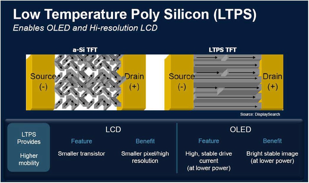
Silicon annealing is a process commonly employed in the semiconductors manufacturing industry. It changes the properties and performance of the silicon chips or wafers as a step in the whole manufacturing process. An example is the use of laser Silicon annealing in the manufacture of Low Temperature Poly Silicon (LTPS) displays. LTPS displays offer optimum customer experience, featuring highest resolution, brightness, colour depth, energy efficiency and as a consequence battery life. They are applicable to the manufacturing of LCD, OLED, curved and flexible displays. In order to achieve all these benefits, the amorphous silicon normally utilised in TFT silicon semiconductor junctions, has to be converted into poly-crystalline silicone (see Figure 1).
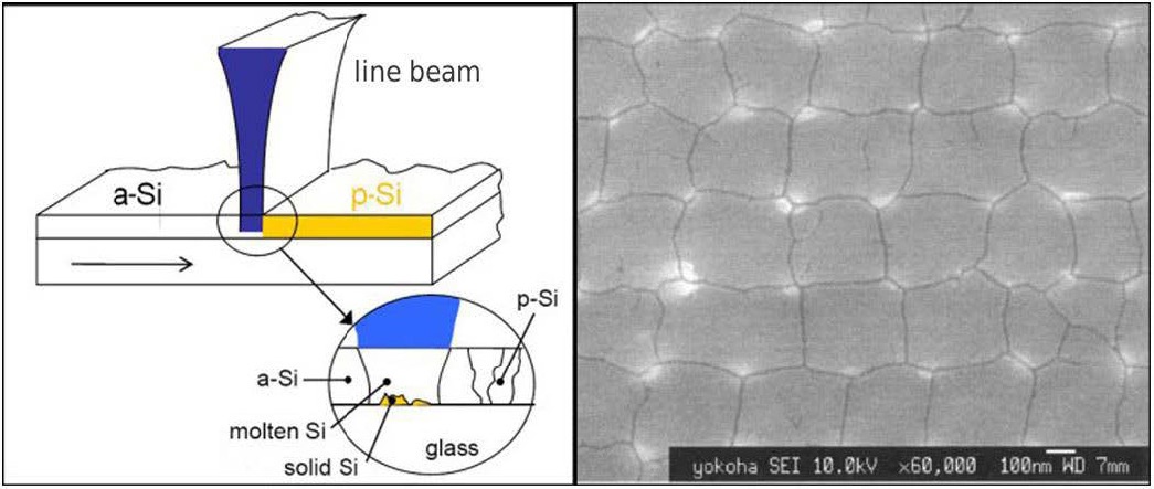
Schematics of crystalline formations of Amorphous Silicon TFT semiconductor junction (left) and Low Temperature Poly Silicon TFT semiconductor junction (right). The process was traditionally performed by Excimer lasers which emit in the UV part of the spectrum. Due to the good absorption of 532 nm wavelength on silicon and the significantly lower cost of ownership of 532 nm DPSS lasers, Powerlase has manufactured the Procyon g2000 laser system. The system produces multiple beams with total power of 2000W, which are then arranged into a line focus of scalable line width of 750 to 1300 mm. The line focus is traversed cross the surface of silicon and anneals the amorphous silicon into polycrystalline silicon (Figure 2). The beam is actually nanosecond pulsed so that it maintains pulse fluence to necessary levels, and all pulses are synchronised within 1 ns trigger variation.


